I-FMD Managed Core Facilities
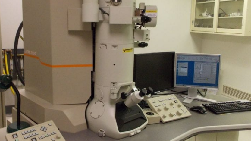
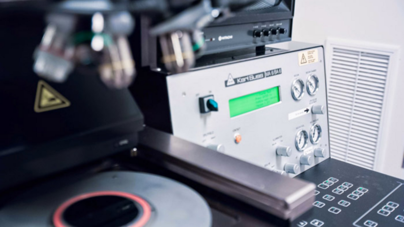
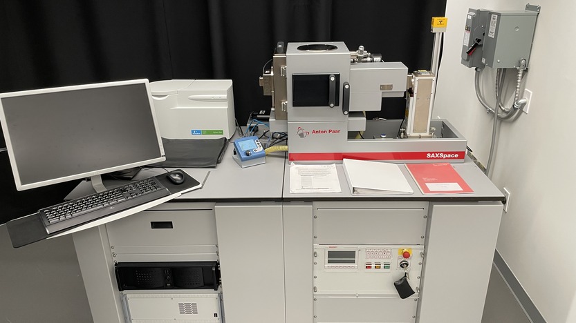
Lehigh University hosts two core facilities for materials research: The Materials Characterization Facility (MCF), and the Integrated Nanofabrication and Cleanroom Facility (INCF).
Both the MCF and INCF are available for use by Lehigh faculty and students as well as external academic, government, and industry partners.
Explore the capabilities of these facilities below and reach out to I-FMD staff if you would like to become a user of any of this instrumentation.