The TEM (JEOL JEM2100 located in WH172C) is useful for phase contrast high-resolution TEM imaging with sub- 0.3 nm resolution and energy dispersive X-ray microanalysis (EDS) with a 5 nm probe size measured full width tenth maximum.
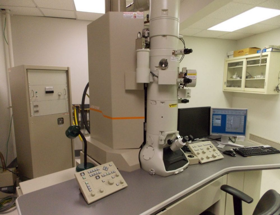
It requires thin samples 3 mm diameter and provides low atomic number X-ray collection (Thermo windowless SDD UltraDry). The electron gun uses a stable LaB6 source automatically controlled by software, and there is a sensitive 2K x 2K CCD camera (Gatan Orius200) to record images and diffraction patterns.
The electron optical system has a wide range of convergence angles and produces excellent convergent beam electron diffraction (CBED) patterns. Sample holders from the atomic resolution microscope also fit right into this TEM that is situated next door to our FIB.
- Minimum accelerating voltage step size is 50 V
- Sample tilt angles range from – 25 to + 25 degrees
- Liquid nitrogen anti-contamination trap
- Typical vacuum during operation 1 x 10⁻⁵ Pa
- X-ray take-off angle 23 degrees with 0.2 str. collection solid angle
- Compatible with Protochips Aduro high temperature heating and Hummingbird Scientific tomography holders.
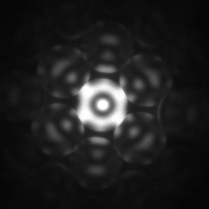
A cubic (110) convergent beam diffraction pattern.
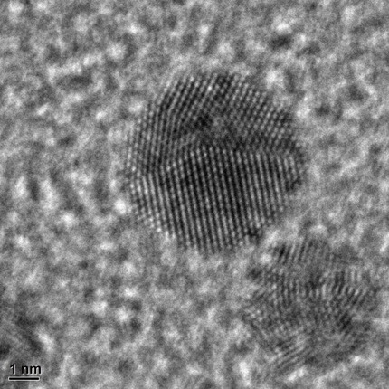
Lattice image showing 0.23 nm spacings in gold nanoparticles, the magnification was calibrated with this image at 800,000 times magnification.