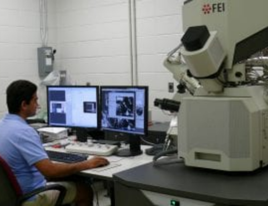
The Thermo/FEI Scios located in WH172B focused ion beam (FIB) is primarily for making cross-section samples for study using SEM imaging and X-ray analysis. This process may possibly be followed by in-situ lift-out, thinning and polishing site-specific samples that are ready for TEM or STEM.
The FIB added new electron back-scattered diffraction (EBSD) and upgraded energy dispersive spectroscopy (EDS) facilities in 2016; it is capable of high speed X-ray analysis in part because it has a bright field-emission electron source (delivering up to 400 nA) and because the silicon-drift EDS electronics (EDAX Ametek) has a high throughput (it can analyze hundreds of thousands of X-rays per second). Rapid X-ray mapping is therefore a major strength of this system.
The instrument boasts an excellent SEM column (ultimate resolution of about 1.5 nm) with both in-lens secondary and in-lens back-scattered electron (BSE) detectors. Other detectors include an Everhard-Thorley (ET) electron detector and a versatile detector capable of collecting ions or electrons (ICE).
The gallium ion column efficiently cuts through materials to reveal sub-surface structure, makes patterns in a surface for optical device applications and facilitates the deposition of an highly localized protective platinum coating or marker. The maximum ion beam current is 65 nA with typical beam energies ranging between 2 keV and 30 keV.
The EBSD system produces accurate crystal orientation measurements and can combine with the EDS system to simultaneously map samples. The sample stage can handle up to 6″ wafers or a large number of standard SEM stubs, it can tilt to 90 degrees; and automated stage control adds the facility to montage large (mm-scale) areas.
- High vacuum operation, option to add liquid nitrogen trapping
- Micromanipulator with integrated motion control
- The FIB is compatible with an Hysitron picoindenter system PI-85
- Built-in plasma cleaner to clean sample and/or chamber
- Navigation camera integrated to facilitate rapid sample movement
- Automated “Slice and View” software to provide 3D dataset
- Beam deceleration technology to optimize low energy SEM
- Transmission Kikuchi Diffraction (TKD) is an available technique.